Custom PCB with 0.1mm Min Line Spacing 1oz Copper Thickness and AOI Test PCBA QC
Product Description:
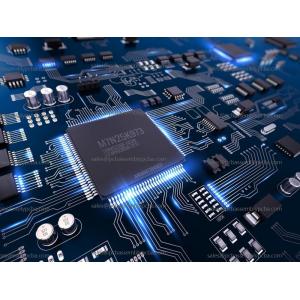
Custom PCB Prototype and Assembly
Our custom PCB prototype and assembly services provide a wide range of solutions for PCBs with layer counts from 2 to 8. We use high-precision flying probe test and E-test to ensure the highest quality of the PCB. The boards are of 1.6mm thickness with 1oz copper thickness. We also perform X-ray, AOI test, and functional test to guarantee the accuracy and reliability of the PCB assembly. Our custom PCB prototype and assembly services are the ideal solution for creating the perfect PCB circuit board and assembly design.
Files and Requirment for PCB,PCBA quotation:
1. A BOM (Bill of Materials) with reference designators: component description, manufacturer’s name and part number.
2. PCB Gerber files.
3. A PCB fabrication drawing and PCBA assembly drawing.
4. Test procedures.

Features:
- Product Name: Custom PCB
- PCB QC: Flying Probe Test, E-test
- Material: FR4
- Solder Mask Color: Green
- Board Type: Custom PCB
- Layer Count: 2-8
- Manufactured by: PCB Assembly Manufacturer
- Assembly Services: PCB Assembly
- Circuit Board Manufacturer: Electronic PCB Assembly
Technical Parameters:
| Parameter | Specification |
| Material | FR4 |
| Min Line Spacing | 0.1mm |
| Min Line Width | 0.1mm |
| Silkscreen Color | White |
| Board Thickness | 1.6mm |
| Copper Thickness | 1oz |
| Layer Count | 2-8 |
| Impedance Control | Yes |
| Solder Mask Color | Green |
| PCB QC | Flying Probe Test,E-test |
Applications:
Custom PCB is widely used in various applications such as electronic products, communication equipment, medical instruments, industrial control systems, automotive electronics, consumer electronics, instrumentation and other fields. It is made of high-quality copper with thickness of 1oz, layer count of 2-8, and minimum line width of 0.1mm. The solder mask color is green, and the PCB QC is tested by flying probe test and E-test. It is suitable for PCB assembly machines, pcb prototype, pcb board print and assembly.
Custom PCB has excellent properties such as high reliability, excellent electrical performance, long service life, good heat resistance, strong corrosion resistance, and good seismic performance. It is the best choice for precise and efficient control of various electrical and electronic products. It can meet the requirements of various complex applications, and can also be used in harsh and special environments. It is widely used in various fields and can provide reliable and stable performance.
Customization:
Custom PCB
We provide custom PCB services to meet your needs. Our PCBs are made with high quality FR4 material. We use Flying Probe Test and E-test to ensure quality of the PCBs. The solder mask color of our PCBs is green. We use X-ray, AOI Test and Functional Test to ensure quality of the PCBA. We provide PCB assembly services OEM and other services.
Support and Services:
PCB,Turnkey PCBA, Electronic Component Souricing, Housing
PCB Assembly, PCBA Manufacturing, SMT, DIP, Testing Service
One stop service, PCB&PCBA, ODM and OEM
Packing and Shipping:
Packaging and Shipping for Custom PCB
Custom PCBs are packaged for shipping based on the size and quantity of the order. For single boards, they are usually placed in a static-resistant bag and then shipped in a cardboard or bubble mailer. For multiple boards, they are usually placed in a larger static-resistant bag and then shipped in a cardboard box.
In order to ensure the safety of the PCBs, all packages are securely sealed and padded for extra protection. The packages are then labeled with the customer's address and a tracking number for easy tracking and delivery.
FAQ:
Q1.What is needed for PCB PCBA quotation?
PCB(printed circuit board): Gerber file and Technic requirements(material, surface finish treatment, copper thickness, board thickness...)
PCBA(printed circuit board assembly): PCB information, BOM, (Testing documents...)
Q2. What file formats do you accept for PCB PCBA production?
Gerber file: CAM350 RS274X
PCB file: Protel 99SE, P-CAD 2001 PCB
BOM: Excel (PDF, word, txt)
Q3. Are my files safe?
Your files are held in complete safety and security.We protect the intellectual property for our customers in the whole process.. All documents from customers are never shared with any third parties.
We are willing to sign NDA effect by customer side local law and promising to keep customers data in high confidential level.
Q4. MOQ?
There is no MOQ in KAIJIN. We are able to handle small as well as large volume production with flexibility.
Q5.Shipping cost?
The shipping cost is determined by the destination, weight, packing size of the goods. Please let us know if you need us to quote you the shipping cost.
Q6. What service do you have?
A: We mainly focus on PCB+SMT+Assembly+Components sourcing service. Additionally, we can also provide injection molding, programming, testing, cables, enclosure assembly service.
Q7. Can we inspect quality during production?
Yes, we are open and transparent on each production process with nothing to hide. We welcome customer inspect our production process and check in house.
Q8. How is your quality?
A: We test both PCB and key components 100% before delivery. Aim to set up long term cooperation with customers. We provide products with reliable quality.
Q9. What is your testing policy and how you control the quality?
For sample, usually tested by flying probe; for PCB Volume over 3 square meters, usually tested by fixture, this will be more faster. Due to there’s many steps to PCB production, we usually do inspection after every step.
20 Years experiences of PCB Assembly, PCBA Manufacturing, SMT, DIP, Testing Service.
Start Inquiry Now!
KAIJIN Precision Manufacturing Co., Ltd.
Address: Crystal Science and Technology Industry, No.51 Xiang Shan Avenue, Ningxi Street, Guangzhou City, China, 511356.
Contact: Rain
Mob(Whatsapp): +86 15918707317
Email: sales@pcbassemblypcba.com
Webside: www.pcbassemblypcba.com