FR4 Tin Spray Epoxy OSP Double-Layer Board PCB Circuit Board with Hard Gold Plating
Product process
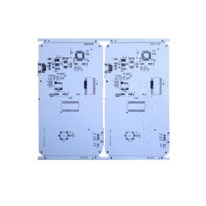
Double-sided PCB board
Double-sided PCB board is a very important PCB board in the circuit board, the market has double-sided circuit board metal base PCB board, Hi-Tg heavy copper foil circuit board, flat winding double-sided circuit board, high frequency PCB, mixed dielectric base high frequency double-sided circuit board, etc. It is suitable for a wide range of high-tech industries such as: telecommunications, power supply, computer, industrial control, digital products, scientific and educational instruments, medical instruments, automobiles, aerospace defense and so on.
The difference between double-sided PCB board and single-sided PCB board
The main difference between double-sided PCB boards and single-sided PCB boards is that single-sided circuitry is only present on one side of the PCB board, whereas double-sided PCBs have circuitry on both sides, with holes in the middle to connect the two sides.
In addition to the production process being different from single-sided PCBs, double-sided PCBs also undergo a copper sinking process, which involves creating a conductive layer between the two sides of the board. This process enables the circuit to be more complex and reduces the risk of signal interference.
The parameters of double-sided PCB boards can vary depending on the specific application, such as the size, thickness, copper weight, and material type. These parameters can affect the performance and reliability of the final product. With their ability to support more complex circuit designs, double-sided PCB boards are widely used in various industries, including telecommunications, automotive, medical, and consumer electronics.
| Copper Thickness | 1oz~3oz,0.5-5 Oz |
| Board Thickness | 1.6mm, 0.5~3.2mm, 0.2-3.0mm, 0.3~2.5mm, 2.0mm |
| Min. Hole Size | 0.25mm, 0.1mm, 0.2 Mm, 0.15-0.2mm, 0.1mm-1mm |
| Min. Line Spacing | 0.003", 4mil, 0.2mm, 0.15mm, 0.1mm4mil) |
| Application | Electronics Device, Consumer Electronics, Electronical Products, Industrial, And So On |
| Layer | 1~20 Layers, 1-24layers |
| Base Material | FR4, Aluminium, TG, Rogers, CEM-1 |
| Min. Line Width | 3mi, 4mil, 0.1mm, 0.1mm(Flash Gold)/0.15mm(HASL), 0.1 0mm |
| Surface Finishing | HASL, OSP, ENIG, HASL Lead Free, Immersion Gold |
| Product Name | Printed Circuit Board, 94V0 PCB Design / PCB Manufacturing |
| Solder Mask | Blue, Green. Red. Blue. White. Black.Yellow, Green/black/white/red/blue Etc., |
| Rohs | Lead free |
| Turnkey PCBA | PCB+components sourcing+assembly+package |
| Assembly details | SMT and Thru-hole, ISO lines |
| Lead Time | Prototype: 15 work days. Mass order: 20~25 work days |
| Testing on products | Flying Probe Test, X-ray Inspection, AOI Test, functional test |
| Quantity | - Min quantity: 1pcs. Prototype, small order, mass order, all OK
|
| Files we need | PCB: Gerber files(CAM, PCB, PCBDOC) |
| Files we need | Components: Bill of Materials(BOM list) |
| Files we need | Assembly: Pick-N-Place file |
| PCB panel Size | Min size: 0.25*0.25 inches(6*6mm) |
| Max size: 20*20 inches(500*500mm) |
| PCB Solder Type | Water Soluble Solder Paste, RoHS lead free |
| Components details | Passive Down to 0201 size |
| Components details | BGA and VFBGA |
| Components details | Leadless Chip Carriers/CSP |
| Components details | Double-sided SMT Assembly |
| Components details | Fine Pitch to 0.8mils |
| Components details | BGA Repair and Reball |
| Components details | Part Removal and Replacement |

Why did you choose us?
1, Experienced
Focused on PCBA electronic manufacturing for 8 years
Best Partner for Listed Companies
Serving over 60 European and American enterprises
Helping clients solve design issues over 500 times
Helped customers solve MP issues over 800 times.
Helping customers improve testing reliability over 1000 times
2, Quality control
ISO9001: 2015
ISO13485
IATF16949
MES
Traceability system
Fully automatic FCT testing
3, Quick response
Quick response principle within 1 hour
7 days * 24 hours
Team responsibility system
Sales personnel with a bachelor's degree or above