High-Precision Prototype PCBs with 0.2mm MinSpace & 0.2mm MinTraceWidth 1.6mm Board Thickness
Product Description:
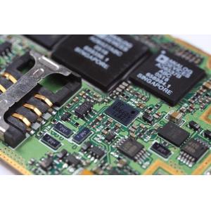
PCB Prototype is a reliable and flexible way to create custom prototype pc boards for various applications. We provide high-quality 4 layer pcb prototype with superior craftsmanship, including 1oz copper thickness, HASL surface finish, green solder mask and 1.6mm board thickness. Our pc board prototypes are highly durable and ensure maximum performance. Our pc boards are designed for quick and easy assembly, making them ideal for prototype and pre-production runs. Our pc board prototypes can be customized to meet your exact requirements and are perfect for a wide range of applications.
Features:
- PCB Prototype Manufacturer:
- Prototype Circuit Board:
- PCB Board Making:
- Quick Turn PCB Prototype:
- Copper Thickness: 1oz
- PCB QC: Flying Probe Test, E-test
- Delivery Time: 3-5 Days
- Board Thickness: 1.6mm
- Min Annular Ring: 0.1mm
Technical Parameters:
| Technical Parameter |
Value |
| Impedance Control |
Yes |
| PCBA QC |
X-ray, AOI Test, Functional Test |
| Copper Thickness |
1oz |
| Board Thickness |
1.6mm |
| PCB QC |
Flying Probe Test, E-test |
| Min Trace Width |
0.2mm |
| Silkscreen |
White |
| Material |
FR4 |
| Solder Mask |
Green |
| Min Annular Ring |
0.1mm |
Applications:
PCB Prototype is a prototype circuit board which is widely used in a variety of applications, and it is usually manufactured by a pcb prototype manufacturer. It mainly consists of two layers and the board thickness is around 1.6mm. The minimum hole size as well as the minimum annular ring are both 0.2mm and 0.1mm respectively. It has high quality standards and goes through rigorous X-ray, AOI, functional and other tests to ensure the quality and reliability. It is a great choice for low cost pcb prototype fabrication, as it is cost-effective and reliable.
Customization:
PCB Prototype Customization Service
Our PCB Prototype customization service offers you with the highest quality and cost effective solutions for your needs. We have the most advanced technologies to provide you with the best surface finish, HASL, and the most precise minimum space, 0.2mm. Our X-ray, AOI Inspection, and Functional Test provide you with the assurance of quality and reliability. Our flexible pcb prototype and prototype pc boards offer you with the perfect impedance control and fast 3-5 days delivery time.
Support and Services:
PCB Prototype Technical Support & Services
At PCB Prototype, we understand the importance of providing quality technical support and services for our customers. We have a team of experienced engineers and technicians available to provide technical assistance and guidance. We also offer a wide range of services to support our customers in the design, development, and manufacturing of their printed circuit board (PCB) prototypes.
Our services include:
- Design consultation and support
- PCB layout and CAD design services
- PCB fabrication services
- PCB assembly services
- PCB testing and quality control services
- Manufacturing and production services
We strive to provide the best quality products and services to our customers, and we are committed to meeting their needs. If you have any questions or need assistance, please contact us and we will be happy to assist you.
Packing and Shipping:
PCB Prototype Packaging and Shipping:
- The PCB Prototypes will be securely packaged in an antistatic bag.
- The bag will then be placed in an ESD safe box.
- The box will be placed in a larger box with enough cushioning materials to protect the PCB prototypes from any possible damage.
- The box will then be sealed and shipped to the customer.
FAQ:
- Q1: What is a PCB Prototype?
- A1: A PCB Prototype is a physical representation of an electrical circuit that is used to test and verify its design. It is often used to evaluate the functionality of the design before full production is started.
- Q2: How long does it take to make a PCB Prototype?
- A2: The time it takes to make a PCB Prototype will vary depending on the complexity of the design, the number of components, and the availability of parts. Generally, a basic prototype can be made in a few days.
- Q3: What materials are used to make a PCB Prototype?
- A3: The most common materials used for PCB Prototypes are copper, solder mask, and silkscreen. Depending on the application, other materials such as flex circuits may be used.
- Q4: What is the difference between a PCB Prototype and a production PCB?
- A4: A PCB Prototype is typically used to test and evaluate a design before full production is started. A production PCB is used when the design is finalized and ready to be manufactured in large quantities.
- Q5: How do I know if my PCB Prototype is working correctly?
- A5: To verify that your PCB Prototype is working correctly, you can connect it to a power source and use a multimeter to measure voltages and currents. You can also use an oscilloscope to view the signal waveforms.